OldDogBlog post 13
In this post I will discuss how I decided on circuit board size and placement of the various components on the ezPixel PCB.
Engineering is frequently an exercise in tradeoffs. I've already made a number of them. For example, I chose to use a BGA package for the FPGA instead of a TQFP. The TQFP was physicall larger, more expensive and had more limited availability at the time I started the design. The BGA is less expensive and physically smaller, allowing for a smaller PCB. But, the BGA is harder to route than the TQFP and a two layer PCB would be harder to accomplish.
The BGA choice also limited the number of FPGA I/O pins I could access. The TQFP would allow me to use 100% of the I/O pins easily. So, tradeoffs.
The schematic was finished up in the previous post. Creating a circuit board from the schematic starts with a netlist. Every schematic capture and layout tool has ways of generating a netlist of component-to-component wire connections and then importing the netlist file into a PCB layout tool. I'm using KiCad and there are numerous tutorials on the interwebs showing examples of how to do this. I referred to those tutorials often as I was learning the tools and keep some of them bookmarked in my browser.
I like to estimate the size of the PCB as an early starting point. The size can always be adjusted larger or smaller as needed, but it is nice to have a target to shoot for. The size and shape of the PCB guide the placement of parts too. Once again simple paper and pencil helped quickly settle on a rectangular shape. Here's how:
The sketch I made of the BGA pinout (OldDogBlog #9 and #11) indicated that the easily accessible pins were grouped around the four corners of the chip. This in turn suggested that there would need to be a level translator and direction select pin – 9 total pins – at each corner. Figure 1 shows a cleaned up block diagram.
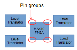
Figure 1: FPGA placement.
Each level translator drives 8 strings so there would be at least 16 x 0.1” header pins along the top and bottom of the FPGA. There were some unused but easily accessible pins along the top and bottom of the FPGA so I could bring some spare pins out as well – always useful to have. I also needed to have pins for external power and ground as this would be one way to power the board. Sprinkle in some extra ground and power pins resulted in 22 pins along each side. 22 x 0.1 = 2.2” as a minimum length along the top and bottom. The sketch looks like Figure 2 at this point.
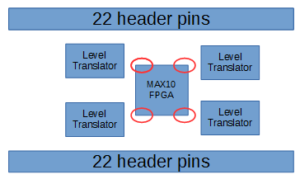
Figure 2. Headers added.
I needed mounting holes in each corner and I decided to put the two pushbuttons along the side so that my fat fingers would have room to actuate both simultaneously. Adding them all up gives about 3” of length along the top and bottom.
The remaining connectors included USB, JTAG and power select. If the JTAG was put at one end between the mounting holes, then the USB and power select could fit at the other end. This makes sense because one source of power is on the USB connector and the other source is some header pins which could be located at that end too. Given the sizes of all these connectors, plus the mounting holes, lead me to an estimate of about 1” wide. Figure 3 shows the result.
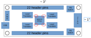
Figure 3. All connectors included.
All that is left is the DC regulator, USB/serial chip and an oscillator and some LEDs and passives. The LEDs and passives are usually pretty easy to fit as they are small. The DC regulator can fit near the power connector and the USB/Serial chip should go right next to the USB connector. The oscillator can find room by the JTAG. The final placement estimate is shown in Figure 4. This is the starting point for a layout.
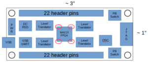
Figure 4: Large parts all placed.
I was able to put all the large components on the top side of a fairly small board which helps keep assembly costs down. An interesting thing to note is that the MAX10 FPGA has power pin decoupling capacitors built into the chip. There is no need to add direct decoupling to each power pin – only power plane bulk decoupling is required. Since the board is so small, I should be able to add the bulk decoupling near the regulator chip. But, being conservative, I decided to add more plane decoupling to the bottom side of the board on the chance that I may need it. These would be “DNI” i.e. Do Not Install, components on the circuit board BOM – Bill of Materials.
This ended the rough component placement stage. The next step is to add the power and ground planes as I described in OldDogBlog #11, then connect all the chip power and ground pins to the planes. I'll pick up there in the next post.
Woof!
Tom Burke
MakerLogic.com