Layout II
OldDogBlog post 14
In this post I will discuss adding the power and ground planes and routing the board.
Kicad makes it very easy to add power and ground planes. I made the top side of the board a ground plane and back in OldDogBlog #11 I showed how I’d need to put a section of ground plane on the bottom of the board to connect to all the ground pins on the inner most section of the BGA grid. Adding sufficient plated vias from the component side ground plane to the back side ground plane ensures the bottom chunk of ground plane would be well connected with ample current capacity. That post also showed a rough idea of how to create power planes on the bottom of the board.
Using planes to distribute power and ground makes it much simpler to connect power and ground pins on the chips as opposed to trying to route power and ground traces all over the place. The planes are also wide enough to handle substantial current if needed. Fortunately, this design is fairly low power. Looking at the current consumption of the various chips suggested that not more than several hundred milliamps of current would be needed at 3.3V or 5V. The FPGA consumption was based on a tool that Intel freely provides along with resource estimates from my early test designs. I used an online trace width calculator to verify that the width of my power planes was more than sufficient for the amount of current that would flow through them. Figure 1 shows the bottom of the board as shown in KiCad. At this point the layout is actually finished because I didn’t think to get a snapshot of it before completing the layout.
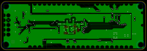
Figure 1: Bottom of ezPixel PCB.
The +3.3V plane is here. The ground plane section is here. The +5V plane is here.
Once the planes are in place my preference is to connect all power and ground pins first. Without those, none of the chips will work. Period. This tends to go quickly because the board is uncluttered – there are no other signal traces that could be in the way. This also allows the traces to the power and ground pins to be as short as I can make them.
Once the powers and grounds were in place, I then focused on
FPGA configuration and JTAG connections. These are crucial to FPGA operation. Without these pins the FPGA will not boot properly and cannot be loaded via JTAG during board production tests. Some of these pins were on inner rows of the BGA matrix and snaking them out resulted in fewer I/O pins being available.
The next signals to contend with are any high speed signals. In my case there is only one clock at 50 MHz and the USB differential pairs between the USB connector and the USB UART chip. I made them as short and direct as was practical. Given that we are only working with USB Low Speed (1.5 MHz) and Full Speed (12 MHz), both of which are not very fast, I decided to forego impedance controlled routing. My reasoning is that the trace lengths would be very short and any impedance mismatch induces ringing would be partly snuffed out because of the signals being differential. Any remaining distortions would likely die out before the middle of the long signal bit periods for USB LS and FS.
Or so I hope…fingers crossed!
The remaining signals are the string drivers, spare FPGA pins, LED and switches and connection to the USB UART. This is where the pin swapping fun starts to happen. Pin swapping occurs when the FPGA I/O pins I picked on the schematic turn out to be too difficult to route easily. Frequently, just changing the chosen I/O pins, i.e. swapping pins, can allow for much simpler and easier signal routing. Fortunately, FPGAs make pin swapping fairly simple.
Figure 2 shows the top side of the board after the layout is complete.
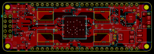
Figure 2: TopSide layout.
The board is essentially ready to be fabricated, but before doing so I always run the pin swaps through the FPGA design tools to ensure it will compile properly. Wouldn’t want to be surprised after the boards were built! I also do a double-check on component availability to make sure everything I need is readily available.
Next up – board fabrication!
Woof!
Tom Burke
MakerLogic.com